Scanning Electron Microscopy
Expert SEM Analysts
Scanning electron microscopy (SEM) is one of the most powerful methods for evaluating engineering materials and understanding how they perform in real world applications. We combine state-of-the-art scanning electron microscopy and microanalysis with a comprehensive level of materials engineering expertise to help clients understand how materials behave. Our engineers apply these extensive SEM capabilities and resources to:
- Identify failure modes such as fatigue, stress cracking, and hydrogen embrittlement
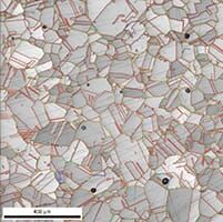
- Evaluate and photograph surfaces, particles, defects, and the structure of engineering materials at magnifications to 100,000X
- Measure the chemical composition of whatever is being examined
- Identify and evaluate the crystalline structure of materials and how manufacturing processes and services influences it
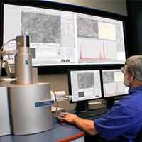
At Stress Engineering Services, highly skilled materials engineers and technologists with decades of industrial and failure analysis experience operate our SEM. Our materials engineers are expert SEM operators who understand engineering materials and interpret SEM results for clients. When engineering support is not required, our technologists operate the SEM and microanalysis system at lower cost for clients who prefer this level of service.
- Large sample chamber accommodating objects 7″ diameter by 5″ tall and weighing up to 18 lbs.
- Live high-resolution projection of SEM images and microanalysis data
- Remote viewing from multiple locations via Internet


