A scanning electron microscope (SEM) uses a focused beam of electrons as the illumination source which is scanned or rastered over the surface of a sample to generate an image. The shorter wavelength of electrons, relative to photons, allows for significantly higher resolution imaging and magnification of a specimen than is possible with light microscopy. Electron microscopy also provides a much greater depth of field than light microscopes, allowing for the imaging of three-dimensional surfaces or objects.
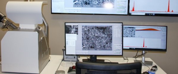
At Stress Engineering Services, we feature the TESCAN VEGA IV Scanning Electron Microscope within our extensive suite of analytical equipment. Our SEM offers advanced “wide field” and “depth” imaging modes, significantly expanding the depth of field compared to traditional secondary electron imaging techniques. Enhancing our capabilities, our SEM can calibrate the stage position using a macro photograph of the sample, enabling seamless mapping of micrographs and spectra during imaging and analysis sessions. It also excels in the collection and analysis of calibrated 3D images, providing accurate measurements of surface features’ height and depth, as well as surface roughness assessments. Additionally, our SEM’s extra-large sample chamber comfortably accommodates samples larger than a standard soda can, underscoring its versatility and suitability for a broad range of applications.

Energy Dispersive X-ray Spectroscopy (EDS)
Our SEM is equipped with a Bruker XFlash® 7 EDS, which allows for the collection of elemental analysis information over a range of working distances for samples of varying heights. The EDS system has variable take-off angle compensation to provide more reliable elemental analyses on rough surfaces similar to the analysis of flat surfaces. In addition, our EDS system has the latest generation of large area detectors, which allows for faster data collection and real-time elemental mapping.
Key Features:
- Large chamber capable of accommodating samples up to approximately 6 inches in diameter and 3.5 inches in height with full X and Y axis travel
- 5 axis (x, y, z, tilt, rotation) motorized stage with 18 lbs. weight capacity
- Stage can be moved into top corner of chamber to allow extra-large specimens to be placed on chamber floor
- Secondary, backscattered, and oblique backscattered electron imaging modes
- 3 nanometers resolution at 30 kV with SE detector
- Accelerating voltages from 5 kV to 30 kV
- 2x to 1,000,000x magnification
- Image size up to 16384 x 16384 pixels
- Dual chamberscopes
- Semi-quantitative EDS analysis with elemental mapping capability
- Expert staff of Materials Engineers, Metallurgists, and Technicians to help evaluate your samples
- Live remote viewing of your samples via Microsoft Teams
Applications:
- Failure Analysis
- Identification of Fracture Modes and Origins – Fractography
- Physical and Chemical Characterization of Surfaces
- Microstructural Analysis
- Digital Image Analysis
- Particle Analysis
- Litigation Support